
Beneq, a global leader in Atomic Layer Deposition (ALD) equipment and solutions, announced Beneq Transmute, a next-generation ALD platform designed for high-volume semiconductor manufacturing. Engineered for high-volume production of Wide Bandgap (WBG) power electronics, advanced RF devices, and μLED and other specialty devices production, Beneq Transmute combines performance, scalability, and cost efficiency in one system.
Atomic precision at manufacturing speed
Beneq Transmute extends the performance of the Beneq Transform XP platform into production environments with the proprietary 3-step ALD architecture. By combining plasma pre-treatment, plasma-enhanced ALD (PEALD), and thermal batch ALD, the platform delivers conformal, high-performance dielectric stacks with atomic-level interface control – now at high throughput.
Its flow-uniform 25-wafer chambers, paired with advanced precursor dosing technology, enable rapid cycle times, optimised wafer coverage, and reduced material waste – resulting in a low cost of ownership across a broad range of semiconductor applications.
“Beneq Transmute represents a major leap forward in making ALD a truly high-volume manufacturing solution,” said Lucas Monteiro, Head of Product at Beneq. “By combining the precision of ALD with throughput and scalability that match production demands, we are giving our customers the ability to produce next-generation Wide Bandgap and RF devices at high throughput and low cost of ownership – with the uncompromised film quality that Beneq is known for.”
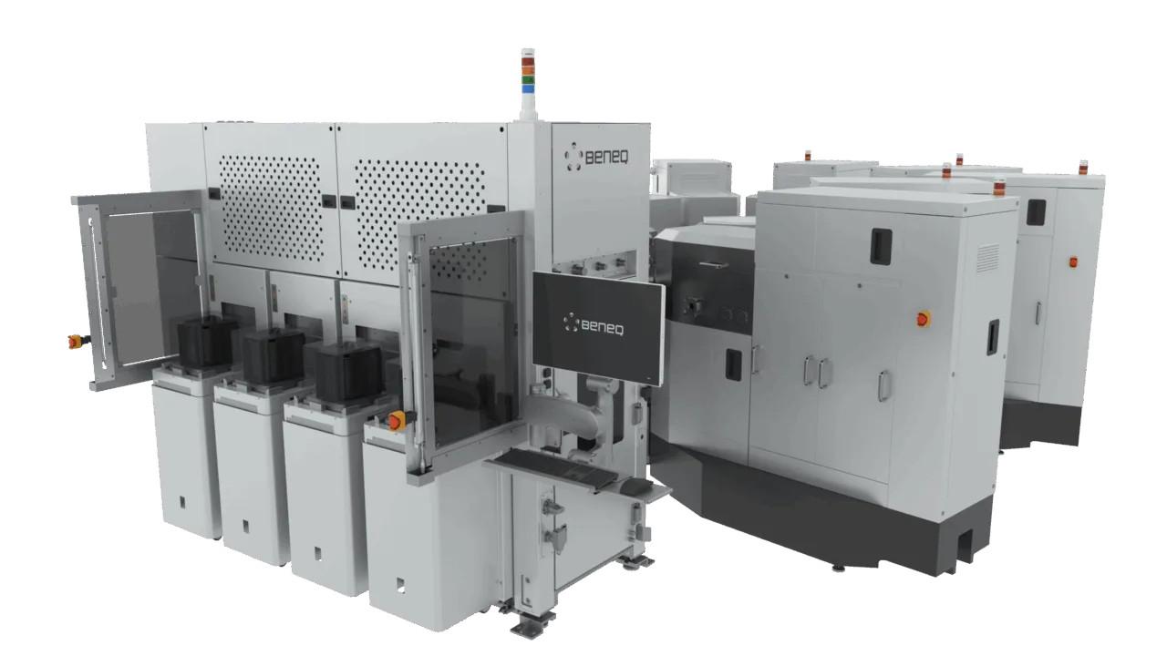
Designed for dedicated production requirements
Beneq Transmute supports both thermal and plasma-enhanced ALD within a modular cluster architecture that enables dedicated configurations. With up to two transfer chambers and eleven process module slots – including PEALD, Thermal, Buffer, and Preheater – each system can be tailored to match specific customer applications and fab roadmaps while ensuring long-term scalability.
Enabling the next wave of electronics
The new solution directly supports key semiconductor market trends – including the electrification of transport, adoption of renewable energy, 5G and RF communications, data centres and next-generation displays. Its combination of atomic precision and production throughput positions Beneq as a technology enabler for a more efficient, connected, and sustainable future.