
DP Patterning and ams OSRAM, a global leader in innovative light and sensor solutions, have developed a joint demonstrator that illustrates how future automotive lighting can be produced more cost-efficiently and with a significantly lower CO₂ impact.
The Open System Protocol (OSP) solution from ams OSRAM provides automotive manufacturers greater freedom in designing and controlling vehicle lighting. Combined with the smart LED driver AS1163, hundreds of light points, sensors, and actuators can be connected through a single continuous line. This creates a simplified electronics architecture of the lighting system that reduces the need for complex multilayer PCBs, enabling the use of DP Patterning’s sustainable printed flexible circuits.
Unlocking new automotive design freedom
“By combining the expertise of ams OSRAM in intelligent LED control with DP Patterning’s flex PCB technology, we unlock new design freedom for automotive interiors. This approach not only adapts to complex shapes but is also paving the way for more sustainable automotive interior lighting elements and effects,” emphasises Andrea Maria Saraceno, Application Engineer at ams OSRAM.
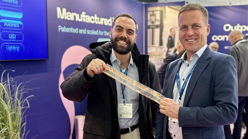
The collaboration has been underway since April 2025 and the demonstrator was showcased for the first time at the productronica trade fair in Munich in November.
“By using our innovative flexible circuits, customers gain a more cost-afficient solution while drastically reducing environmental impact. We are very pleased that ams OSRAM has demonstrated a concrete way of applying our circuits in a smart, energy-efficient solution. We are now looking for more partners from various industries, who are interested in exploring the possibilities through pilot projects and hopefully scaling production together. The potential is enormous,” says Staffan Nordlinder, CEO of DP Patterning.
Sustainable and cost-efficient electronics
The major environmental advantage of DP Patterning’s flexible circuits lies in the manufacturing process. The patented Dry Phase Patterning (DPP) replaces traditional wet etching with a dry, chemical-free method. By mechanically patterning the metal layer instead of using chemicals, the environmental impact of the manufacturing process is reduced by up to 98 percent. Switching from expensive silver to aluminium, a far more abundant and affordable material, significantly reduces the material cost. Faster production speed and easier handling of finished products make the process even more cost-efficient.
Scalable production
Developed and refined in Norrköping, Sweden, DP Patterning’s technology has evolved into a scalable solution for sustainable electronics manufacturing. Today, DP Patterning supplies flexible and sustainable PCBs to leading companies worldwide across industries such as automotive, consumer electronics, communications, MedTech, aviation and industrial solutions. The next step is to establish easily installed micro-plants designed for regional, high-volume production, which will bring the manufacturing closer to the customer.