
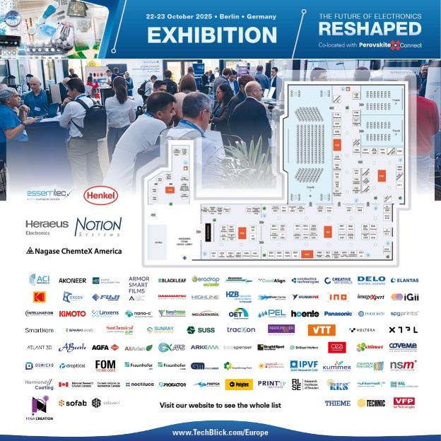
TechBlick’s The Future of Electronics RESHAPED conference and exhibition (22 & 23 October 2025, Estrel Berlin) is just days away! It is poised to welcome over 100 invited speakers, 95 exhibitors, and 600 participants from around the world.
This year’s agenda once again covers the state-of-the-art across the full innovation spectrum of additive, sustainable, printed, hybrid, R2R, 3D and wearable electronics.
In this article, we introduce the conference agenda, highlighting innovations that will be showcased as part of the conference programme.
The conference – an overview
Akoneer: Laser-processed multilayer glass PCBs for semi additive semiconductor packaging. Demonstrating high-density interconnections on glass substrates.
Antolin: Dynamic automotive interiors using E Ink Prism trim surfaces.
Armor Smart Films: Using piezoelectric coatings to enable sensors, haptics, heating, and medical devices.
Auburn University: Developing thermoformed IME circuits that replace wire harnesses and enable driver monitoring sensors.
Blackleaf: Enabling efficient thermal control with graphene heating inks for flexible foils and coatings.
CEA-Leti: Optimising additive PCB fabrication to replace subtractive methods and enable sustainable electronics.
CondAlign: Using particle alignment to develop anisotropic films that cut filler use and cost.
CurveSYS Sensors: Enabling security sensing with flexible pressure arrays that differentiate impacts in real time.
DELO: Using high-barrier encapsulants to extend perovskite PV lifetimes and efficiency.
Eastman Kodak: Enabling scalable printed circuits by shifting from screen printing to high-resolution flexography.
ELANTAS Europe: Developing functional pastes to enable flexible, durable in-mould automotive electronics.
Enjet: Enabling high-throughput deposition with EHD multi-nozzle printing for viscous functional inks.
Fraunhofer EMFT: Using roll-to-roll UV lithography to enable seamless, high-resolution flexible circuits.
Fraunhofer ILT: Optimising conductivity by developing selective laser sintering for stable printed sensors.
Fraunhofer ISE: Enabling sustainable perovskite PV by addressing toxic solvents and critical materials.
Fuji Corporation: Inkjet-printed silver nano-inks on UV-curable substrates for multilayer circuits with embedded components.
GE Aerospace: Enabling aerospace resilience with additive RF sensors and packaging rated to 1000°C.
Hamamatsu: Developing NIR laser sintering for greener, energy-efficient printed electronics.
Heraeus Electronics: Developing polymer thick-film conductors with improved solderability and thermal stability.
Heliatek: Enabling certified lightweight flexible PV with R2R multilayer deposition.
Henkel: Using silver/copper inks to enable hybrid integration and 3D functional electronics.
HighLine Technologies: Scalable microextrusion of silver and other materials with fine lines <20µm at >500mm/s for metallization.
Holst Centre: Enabling recyclability in IME through closed-loop recovery of plastics and metals.
Hummink: Using capillary printing to enable nanoscale (100 nm–50 µm) additively-manufactured interconnect, bumps and biosensor printing.
iGii: Developing 3D carbon nanomaterials with scalable R2R processes for POC diagnostic devices.
Intellivation: Enabling flexible PV by using R2R sputtering for barrier and conductor films.
Karlsruhe Institute of Technology: Enabling sustainable interconnections with copper busbars and low-Ag metallization pastes.
Mesoline: Microchannel particle deposition (MPD) for wafer-scale micron-precision material placement.
Myrias Optics & UMass Amherst: Enabling wafer-scale metaoptics by using nanoimprint lithography with nanoparticle inks.
NanoPrintek: Enabling inkless nanoparticle-based dry printing without sintering using laser particle generation and in-situ laser sintering.
OET Energy / Coatema: Scaling printed PV by enabling Giga Fab production with R2R and AI.
Hoenle Adhesives: Using adhesives to enable solder-free, durable encapsulation for flexible devices.
Panasonic: Enabling slimmer, tougher devices with self-healing Toughtelon films.
Perovskia Solar: Scaling digitally printed PV to 1M units for IoT and consumer devices.
Prio Optics: Enabling anti-reflective and optical coatings through additive inkjet printing.
RISE: Enabling stretchable circuits with screen-printed liquid metal inks.
SATO Global: Using RFID digital twins to enable real-time manufacturing intelligence.
Signify Research: Enabling novel lighting form factors and more sustainable devices by printing LEDs on flexible foils.
Silicon Austria Labs: Optimising circularity in printed electronics with LCA-driven design strategies
Sofab Inks: Enabling scalable perovskite PV with soluble, cost-efficient formulations.
SOLRA-PV: Printing encapsulated perovskite solar modules for battery-free IoT and consumer devices.
Sonojet: Using SAW-based aerosol printing to enable clog-free, tuneable deposition.
SparkNano: Enabling gigawatt PV by scaling SnO₂ ETL deposition with R2R ALD.
Sunray Scientific: Developing UV-cured anisotropic epoxy to enable fine-pitch interconnects.
Toyota: Cross-industry innovations incl. SMA wire actuators with feedback, NIR pigments for hidden data transfer, and metamaterial vibration damping for electronics.
TracXon: Enabling additively manufactured high-density double-sided circuits with patented R2R printed VIA fabrication.
Trusscore: Using electrochromic PVC to enable colour-changing wall panels.
TU Dresden: Enabling eco-flexible electronics with biosourced leaf-based substrates.
University of Coimbra: Developing liquid metal composites to enable recyclable, repairable electronics.
University of Glasgow: Enabling sustainable monitoring with chip-free, battery-free RF sensors.
University of Manchester: Using graphene inks to enable multifunctional printed devices and heaters.
University of Rome Tor Vergata: Enabling fully printed perovskite PV with ambient processing and >1000 h lifetimes.
Valeo: Integration of printed and in-mould electronics into vehicles addressing specs, resources, and quality demands for next-gen automotive adoption.
Wiliot: Battery-free Bluetooth IoT tags produced R2R with printed sensors.
Würth Elektronik: Optimising PCB sustainability with selective solder masks and recyclable bases.
X-Fab: Enabling heterogeneous integration via micro-transfer printing of ultra-thin chiplets.
Lockheed Martin: Case study on flexible hybrid electronics (FHE) adoption, incl. copper additive manufacturing and flexible RF circuits.
Solaires Entreprises: Developing slot-die and blade-coated perovskite modules for scalable PV.
Q5D: Enabling 3D metallization by using 5-axis laser-assisted processes.
XTPL: Developing ultra-precise dispensing to enable bonding and defect repair.
AMAREA Technology: Enabling ceramic components with integrated electronics via multi-material 3D printing.
Lithoz: Co-printing dielectric ceramics with Cu/Ag for functional multi-material electronic components.
INO: Enabling smooth R&D-to-production scaling with modular screen-printing lines.
NGK Europe: Ultra-thin, semi-solid Li-ion batteries with ceramic electrodes to enable safe wearables and IoT.
NRC Canada: Using volumetric additive electronics manufacturing to enable rapid 3D overprinting of conductors.
Notion Systems: Enabling high-viscosity deposition by advancing EHD printing beyond inkjet.
ImageXpert: Optimising inkjet adoption by enabling structured printhead evaluation.
Printed Electronics Limited: Viscous-jet deposition for highly loaded functional inks (>5k cP) enabling digital drop-on-demand printing of inks previously restricted to screen processes.
NextFlex: Enabling commercialisation of AME through a 200+ partner ecosystem.
Helmholtz-Zentrum Berlin: Enabling scale up of solution-processed perovskite PV with standardised data handling and metrology.
CEA: Low-T printing, interface advances and long-term encapsulation for upscaling Si-perovskite tandems
Ceradrop (MGI Digital Technology): Enabling agile PCB and etching production with digital additive manufacturing.
DR Utilight: Developing laser pattern transfer printing to enable 10μm PV lines or 20µm solder bumps.
Conductive Technologies: Enabling high-performance sensors by optimising material stack-ups.
GraphEnergyTech: Using carbon inks to enable scalable, low-resistance printed electronics.