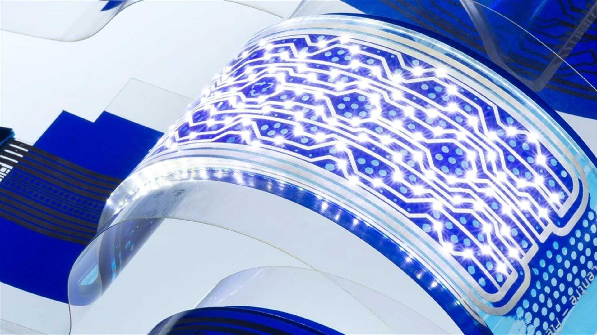
Increasingly, electronics are being integrated with plastics to form a seamless unit with the product, from automotive parts to consumer electronics and medical devices. This results in lighter, more aesthetically pleasing and cost-efficient products. But this integration complicates recycling and repair. TNO at Holst Centre developed a new disassembly method that allows electronics to be detached from the carrier at the end of the product’s life, enabling recycling and repair. This innovation contributes to future efficiency and cost savings in business, while reducing CO2 emissions and electronic waste. Initial research results were recently published in the Journal of Cleaner Production.
Printed electronics
Companies are increasingly using printed forms of electronics because they can be seamlessly integrated into almost any product. Mechanical buttons and switches are not necessary; they are printed. As a result, the electronic part weighs less and the product has a nicer design. In addition, it is easier and faster to produce. Many applications are conceivable, for example in wearable medical sensors, car dashboards, aircraft control panels or industrial machinery, as well as in washing machines and coffee makers. It is estimated that the market size of this technology will increase from about $175 million to more than $3 billion between 2022 -2032.
Recycling and repair
In this technology, to protect the electrical circuitry, the electronic components and printed metals are fused with plastics. This makes repair and recycling virtually impossible. Currently, for these types of electronics at the end of life only the shredder and incinerator remain. This leads to CO2 emissions, and unnecessary loss of burned raw materials. Only one-fifth of all electronic waste worldwide is currently neatly recycled. The amount of electronic waste is estimated to reach 74.7 million tons by 2030 and 110 million tons by 2050.
Water-based layers
To dismantle this printed form of electronics, TNO developed a special water-based layer. This was applied between the circuit with components and the outer plastic layer of the electronic test device. Tests showed the layer was strong enough to withstand 1000 hours of humidity up to 85% and a temperature of 85 degrees Celsius. At the same time, the new layer is flexible enough to remove the plastic without damaging the electronic circuitry. If products were found to be defective during testing, they were taken apart and repaired. Then the device was covered with plastic again and the electronics worked as they should.
Better for economy and environment
This method allows printed electronics to be repaired and fully recycled, which was previously not possible because of the fusing of electronics with the plastic. It allows companies to repair design errors during production, leading to cost savings and more efficient use of materials. It will also improve recycling, reduce waste and enable more sustainable production methods. This allows companies to bring new products to market that already comply with future European Commission rules on sustainable design (Ecodesign for Sustainable Products Regulation).
Caption: After the electronic device was detached, it was again covered with plastic and the electronics worked as they should


