
In flexible and printed electronics, the real challenge is not imagining new device concepts. It is validating them fast enough to matter. Whether the application is a flexible display, smart packaging, or thin-form energy storage, development teams need to assess how materials interact, how multilayer structures hold up, and how quickly a prototype can move from first print to meaningful iteration.
That makes prototyping one of the most important pressure points in the development cycle. Flexible electronics is not just about printing on a bendable substrate. It is about combining conductive, dielectric, adhesive, and other functional layers into structures that perform reliably and can eventually support manufacturing. In practice, success depends on how quickly teams can test compatibility, refine stackups, and repeat the process with confidence.
The reality of prototyping flexible electronics
During the prototyping stage, teams must evaluate whether a given ink is compatible with a chosen substrate, whether the dispensing process produces stable and repeatable features, whether a multilayer stack can be aligned and built up successfully, and whether the resulting structure can point toward a process that is manufacturable at scale.
These requirements create a number of practical bottlenecks. Inkjet systems, for example, can achieve very fine trace widths, sometimes down to 50 μm, but they often struggle with highly loaded conductive materials because those materials are more likely to clog nozzles. Other methods may support thicker or more viscous materials, but they introduce different tradeoffs in process control, throughput, or layer definition.
The success of a flexible electronics prototype, therefore, often depends less on a single device idea than on the versatility of the platform used to develop it. Whether the end goal is a flexible display, a printed battery, or a smart packaging device, teams need a system that can handle a broad range of materials and substrates while also supporting the repeated trial-and-error that meaningful R&D requires.
NOVA: A materials dispensing system for prototyping flexible electronics
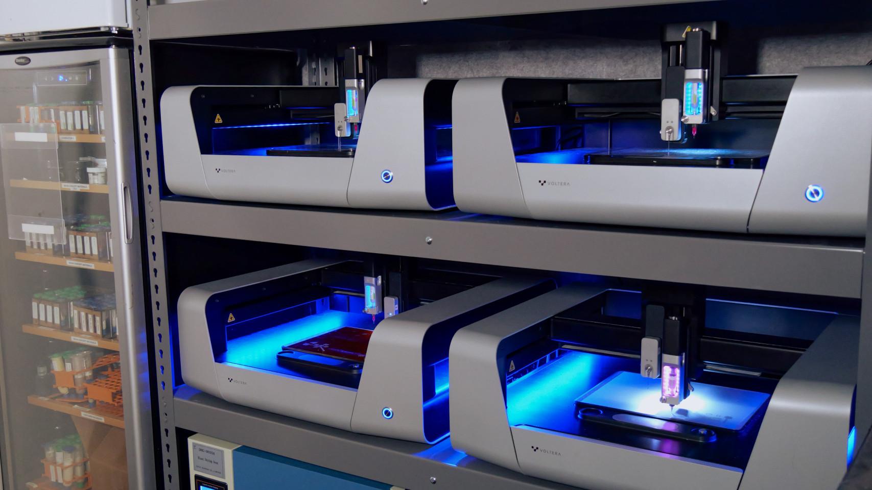
Voltera is a Canadian company that develops rapid prototyping platforms for electronics development. Recognised with awards including the James Dyson Award and the GOOD DESIGN Award, Voltera’s systems are used by organisations such as NASA, MIT, and Harvard University. Researchers have been using Voltera’s machines to publish in journals such as Nature, Advanced Materials, and Flexible and Printed Electronics.
NOVA is designed to accelerate flexible hybrid electronics R&D. It uses direct ink writing technology to dispense screen-printable materials with viscosities ranging from 1,000 to 1,000,000 cP across a wide variety of substrates, and it is optimised for multilayer circuit development. In practice, this means NOVA can work with most of the materials that matter in the production stage, compared to other digital deposition approaches like inkjet.
NOVA’s dispensable materials include conductive inks such as silver, copper, gold, and carbon, as well as conductive polymers, dielectric materials, solder pastes, adhesives, and other functional materials. Supported substrates include flexible materials such as polyimide, PET, PETG, polycarbonate, and silicone; stretchable materials such as TPU, cotton fabric, BEYOLEX, and Evolon fabric; porous materials such as paper and plywood; and rigid materials such as FR1, FR4, glass, alumina, ceramic, PET-CF, Rogers PCB materials, and Soluboard.
Since its launch in 2022, NOVA has helped users around the world tackle meaningful challenges in printed electronics, from electronic skin research to space-related applications. Beyond customer use, the Voltera team has developed a series of internal projects that help illustrate the role additive prototyping can play in flexible electronics R&D.
Printing flexible circuits with NOVA
Below are some NOVA projects completed by Voltera’s team relevant to the current direction of the flexible electronics industry: a multilayer flexible battery, a flexible electroluminescent display, and an RFID tag for smart packaging integration.
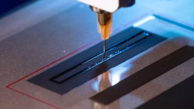
Flexible battery project
Energy storage is where flexible electronics often run out of road: a device can be thin and conformal until it needs a battery, and then the form factor is forced back into a rigid box. This is why printed and thin-film batteries remain a central research focus.
Voltera used NOVA to fabricate a seven-layer magnesium-zinc battery on flexible PET, dividing the device into two laminated halves and printing conductive, electrode, separator, adhesive, and electrolyte layers in sequence. The resulting device delivered about 2.4 V, showed an initial capacity of about 1 mAh, and reached a final printed thickness of roughly 500 μm, excluding the substrate. More importantly, the project illustrates how additive battery prototyping allows teams to evaluate not only chemistry, but also deposition behaviour, layer leakage, drying, lamination, and form factor much earlier in development.
Flexible display project
The flexible display landscape spans multiple technologies, and prototypes often require both display-layer experimentation and display-adjacent circuitry that must flex, conform, or integrate into non-planar assemblies.
Using NOVA, Voltera’s team printed a blue electroluminescent pattern on both PET and cardstock paper by building a four-layer stack consisting of a base conductive layer, dielectric layer, phosphor layer, and top conductive layer. Once driven with alternating current, the printed structure emitted an even blue glow, validating a multilayer process for translating a display concept into a working device on both flexible and porous substrates.
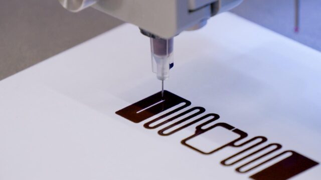
RFID tag project
Smart packaging often starts with a simple requirement to identify, track, or authenticate an item, but quickly becomes a multidisciplinary challenge spanning substrate sustainability, antenna performance, attachment/integration, and manufacturing cost.
For smart packaging, Voltera’s team used NOVA to print an ultra-high-frequency RFID tag on paper using copper ink. Because the design could be tuned and refined in only a few iterations, it highlighted one of the main advantages of additive prototyping for smart packaging: the ability to quickly test antenna geometry, material behaviour, and substrate compatibility without waiting on tooling or external manufacturing cycles. The performance of the RFID tag exceeded that of off-the-shelf RFID tags from market leaders, demonstrating how printed electronics can be integrated onto packaging-friendly substrates while still meeting key electrical requirements.
In flexible electronics, success depends on more than proving that an idea can work once. It depends on building a repeatable path from material evaluation to functional prototype, and from early prototyping to production-ready thinking. Voltera’s focus is to make that path more accessible, helping teams reduce friction, iterate faster, and move promising concepts forward with greater confidence.