
Laser sintering is a relatively new technology that uses lasers as efficient thermal energy sources for sintering metal particle-based inks. Semiconductor-based near-infrared (NIR) lasers wield several advantages over traditional methods, such as hot air ovens and flash lamp ovens, in sintering printed electronics.
Semiconductor lasers are highly energy-efficient and have long lifetimes that exceed 20,000 hours. They are also environmentally friendly. This is evident in their low energy consumption, minimal use of consumables, and reduced servicing requirements. These same factors also lead to considerable savings in operational costs and uptime for end users over the lifetime of the printing equipment. Laser sintering solutions have a smaller footprint than conventional ovens and can be easily scaled up in power for higher throughputs. NIR lasers are especially suitable for thermally sensitive substrates like polymers, which have minuscule NIR absorption compared to the inks. The same cannot be said for conventional ovens that also heat the print substrates to high temperatures. These and other advantages of laser sintering have often been discussed [1,2].
Exploring the potential of laser sintering in the printed electronics industry
Hamamatsu Photonics has been assisting the printed electronics industry to explore the potential of laser sintering to their advantage [3,4,5]. They have worked closely with several ink suppliers and printed electronics manufacturers to optimise laser sintering parameters in their application lab [5] and at their partner sites. Since laser sintering is a novel technology, its performance in real-world situations must be demonstrated with unbiased tests.
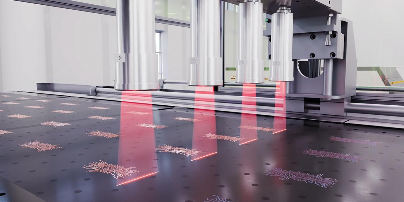
To achieve this, Hamamatsu’s engineers partnered with researchers at Fraunhofer Institute for Electronic Nano Systems to create realistic high-volume printing conditions [6]. Specifically, the test conditions were set to simulate high-speed roll-to-roll (R2R) printing on an inkjet printer using silver nano-inks. The printing conditions were optimised for the inks used without considering the downstream sintering method, therefore laser sintering was not favoured in these tests.
Both laser line illumination and scanning spot illumination were employed for sintering at printing speeds of 1.5-6.0 m/min. Remarkably, even with only a fraction of the laser power used, high conductivity of up to 2.22 × 10⁷ S·m−1 was achieved in sintered products within a few seconds. This represents 36% of the bulk conductivity of silver, which is considered an excellent result in printed electronics. The results also indicate that laser line illumination is highly suitable for continuous printing, whether sheet-fed or R2R.
Peer-reviewed publication
For more detailed information, Hamamtsu Photonics invite readers to access the peer-reviewed publication, which is freely available [6]. It is important to note that higher laser powers can potentially increase the throughput without any changes to the hardware footprint, making laser sintering a future-proof solution for end users.
Hamamatsu Photonics is keen to collaborate closely with the printed electronics community and support industry stakeholders in trialling laser sintering. Please reach out to their team of experts at info@hamamatsu.eu to discuss how this could impact your business.
Overall, the promising results and ongoing development of laser sintering technology highlight its potential to revolutionise the printed electronics landscape, making it a critical area for future exploration and innovation.
References:
[1] E-Paper – “Increasing production efficiency of printed electronics manufacturing with laser sintering” PRO Flextronics Media Hub vol 3, 2025, Smart living & mobility, p20: https://m2n-converting.com/epaper/pro-flextronics-no-3/#1
[2] Hamamatsu Photonics, “Weld, Solder, Cure or Sinter with SPOLD® LD irradiation light source” [online]: https://www.youtube.com/watch?v=I0sLZBR9u_I
[3] Hamamatsu Photonics, Applied products of semiconductor lasers [online]: https://www.hamamatsu.com/eu/en/product/lasers/applied-products-of-semi-conductor-lasers.html
[4] Hamamatsu Photonics, “Laser Sintering – a sustainable and rapid post-process for high volume production”, TechBlick [online]: https://youtu.be/xNtAtrEn-Krk?feature=shared
[5] Hamamatsu Photonics, “Lasers for sintering of metal particle based inks in Printed Electronics”, TechBlick [online]: https://www.youtube.com/watch?v=-jDpdcXOOwc0
[6] Mitra, D.; Mitra, K.Y.; Buchecker, G.; Görk, A.; Mousto, M.; Franzl, T.; Zichner, R. Laser Sintering by Spot and Linear Optics for Inkjet-Printed Thin-Film Conductive Silver Patterns with the Focus on Ink-Sets and Process Parameters. Polymers 2024, 16, 2896. https://doi.org/10.3390/polym16202896