

According to a market research report [1], the global wearable medical devices market is on pace to more than double from USD $103.1 billion in 2026 to USD $229.9 billion in 2033. Smart sensors, the backbone of connected city infrastructure, are tracking a similar curve, expected to climb from about USD $59.8 billion in 2026 to USD $169.8 billion by 2030 [2].
These two fastest-growing corners of electronics have very different end products but the same underlying appetite: more sensors, conforms more to the contours of the human body, or embedded deeper into everyday infrastructure. Both are pushing electronics into places, shapes, and capabilities that conventional prototyping methods are not built for.
Two trends, one problem
For hardware teams, that shift shows up as pressure in a specific place: development. A wearable device that has to sit against the skins for a full day and stretch with the body movements needs materials that a rigid PCB workflow simply cannot validate. A sensor or control panel destined for a moulded, three-dimensional surface needs to survive being formed after it’s already a working circuit.
Because both trends are moving faster than standard materials catalogues can keep up, teams increasingly find themselves formulating their own inks rather than waiting on a supplier’s roadmap. Testing all three, skin-safe materials, formable circuits, and custom formulations, usually means juggling several disconnected tools and processes, which slows the exact iteration these markets are rewarding speed for.
Where Voltera’s NOVA materials dispensing platform fits
Voltera is a Canadian company that develops rapid prototyping platforms for electronics development. Recognised with awards including the James Dyson Award and the GOOD DESIGN Award, Voltera’s systems are used by organisations such as NASA, MIT, and Harvard University.
NOVA, Voltera’s materials dispensing system for flexible hybrid electronics, was built with exactly this kind of shifting ground in mind. Using direct ink writing, it dispenses screen-printable materials across a viscosity range of 1,000 to 1,000,000 cP, onto substrates spanning flexible, stretchable, porous, and rigid categories.
Wearables that sense continuously, and act remotely
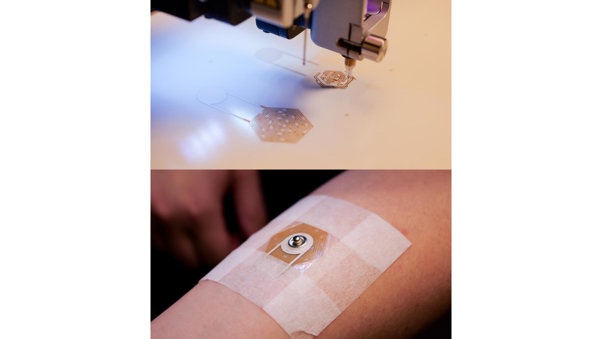
Title image (Fig.1): Top: NOVA dispensing gold ink to make ECG electrodes. Bottom: One electrode conforming to a person’s arm.
Voltera’s Applications team used NOVA to print a set of dry ECG electrodes directly onto TPU, replacing the wet gel electrodes still standard in most clinical settings. Inspired by published research into optimised dry-electrode geometry [3], the design used a hexagonal labyrinth pattern to maximise skin contact while avoiding the irritation gel electrodes can cause over long wear. A stretchable silver base layer carried the mechanical flex, while a thin biocompatible gold layer, applied sparingly to manage cost, handled the skin-contact surface. Connected to a heart rate monitor and microcontroller, the finished electrodes captured a clean, continuous ECG waveform: a proof of concept, not a diagnostic device, but one that demonstrates the kind of long-duration signal fidelity continuous monitoring increasingly needs to deliver outside a clinic.
A related project pushed wearable sensing toward action rather than just measurement. The team printed stretchable strain-gauge traces onto TPU in a meandering pattern for extra sensitivity, then laminated them into an off-the-shelf glove. As the wearer’s fingers bent, the changing resistance was read by a microcontroller and transmitted wirelessly to a second board driving a set of servos, letting a 3D-printed robotic hand mimic the glove’s movements in real time, closing 60 degrees at the fingers, enough to grip a mug. The same wearable-sensing approach that supports diagnostics also supports teleoperation, with applications in prosthetics and remote handling in hazardous environments.
Interfaces built into the surface itself
The same pressure toward integration is reshaping how cities and connected products handle human interaction. Instead of discrete switches and buttons, more control interfaces are being moulded directly into product and infrastructure surfaces, an approach known as in-mould electronics. Voltera’s team prototyped this end to end with NOVA, across four stages: printing the sensor circuit, building a custom-designed forming tool, thermoforming the printed part, and printing a separate interface board to complete the system.
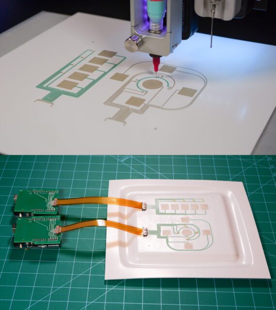
Fig.2: Top: NOVA dispensing dielectric ink. Bottom: The moulded circuit connected to the Arduino Uno controllers. (c) Voltera
The sensor itself was a capacitive touch circuit, including a slider and a circular control, printed on ABS with a conductive base layer and a dielectric top layer that both insulated the traces and reinforced them mechanically ahead of forming. The team then designed and 3D printed a custom buck, accounting for draft angle and expected material stretch, and used it with a thermoformer to shape the printed circuit into its final three-dimensional geometry.
Once wired into an Arduino-based control system, both the slider and the circular control responded reliably to touch, with LEDs providing immediate visual feedback. That sequence, print first and form second, is what makes in-mould electronics practical for kiosks, panels, and other shared infrastructure where a flat add-on switch isn’t an option, and it depends on validating the printed circuit’s survival through forming before ever reaching a production tool.
NOVA for functional ink development
Underneath both trends sits a category of work that increasingly draws attention from innovators: functional ink development. A functional ink is a material engineered to deliver a specific property, conductivity, insulation, adhesion, or luminescence, and its performance depends on getting particle size, solids content, and viscosity right for both the printing process and the end application. When no off-the-shelf formulation hits the target, teams have to build the ink themselves, which turns prototyping into a two-part problem: validating the device and validating the material it depends on, at the same time.
Voltera took this on directly, developing a custom carbon-based resistive ink from raw components: carbon black for conductivity, a polymer binder for adhesion and particle dispersion, and a solvent blend tuned for evaporation rate and nozzle compatibility. The formulation targeted resistance between 600 and 6,000 ohms, suited to a potentiometer application, while holding a viscosity around 1,500 cP for smooth dispensing. The finished ink printed cleanly onto PET and performed exactly as designed, smoothly dimming a connected LED circuit as the printed wiper moved along the resistive trace.
The same underlying capability extends well beyond one potentiometer. Functional ink development spans conductive metal-based inks, carbon-based and polymer formulations, and specialty ceramics, feeding directly into the sensing layers wearable health tech depends on and the printed circuitry embedded in smart infrastructure. Being able to formulate, print, and test a candidate ink in the same afternoon, rather than waiting weeks on an outside supplier, is often what determines whether a new material makes it into a device at all.
Where this leaves development teams
Wearable health tech and smart-city infrastructure will keep pulling electronics into tighter, less conventional spaces, and often into materials that don’t exist yet on a catalogue page. Voltera built NOVA to close that gap, from validating a finished device to formulating the ink it runs on.
References:
[1] Grand View Research. Wearable Technology Market (2026 – 2033). https://www.grandviewresearch.com/industry-analysis/wearable-technology-market.
[2] Grand View Research. Smart Sensors Market (2024 – 2030). https://www.grandviewresearch.com/industry-analysis/smart-sensors-market-report.
[3] Francis, P., Dhanabalan, Shanmuga Sundar, Robel, M. R., Elango, S. P., Walia, S., Sriram, S., & Bhaskaran, M. (2023). Dry electrode geometry optimization for wearable ECG devices. Applied Physics Reviews, 10(4). https://doi.org/10.1063/5.0152554.