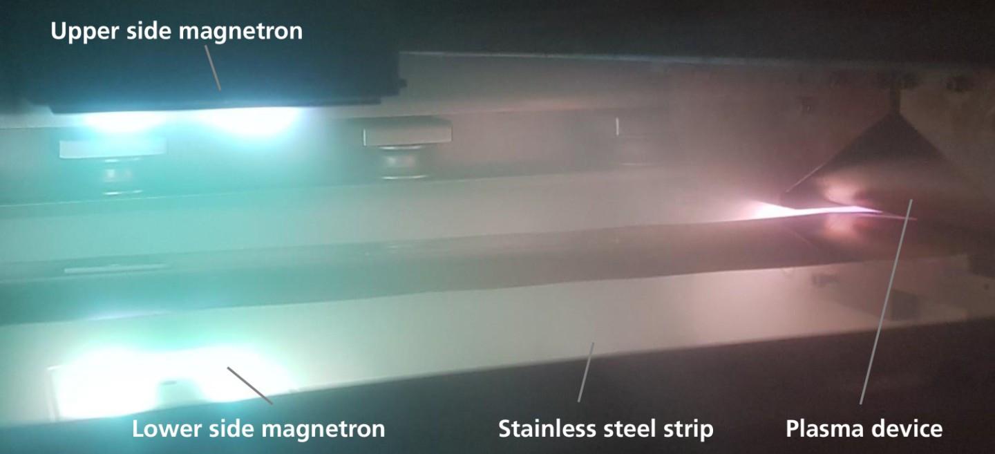
Graphene layers promise great progress and increased efficiency in solar applications, energy storage and smart glass applications due to their outstanding properties, including transparency, barrier effect and conductivity. The lack of scalable deposition processes with consistently high layer quality at cost-efficient throughputs has so far prevented the breakthrough of this promising material. As part of the funded EU project NewSkin (GA No. 862100), the Fraunhofer Institute for Electron Beam and Plasma Technology FEP has developed an innovative PECVD process that enables the deposition of graphene at high process speeds and offers higher production throughputs and a wider range of substrates at lower process temperatures.
Graphene has the potential for outstanding performance gains in solar cells, organic light-emitting diodes (OLEDs), electrical energy storage devices or smart windows and even membranes, e. g. for seawater desalination. Its phenomenal properties are impressive: the material is transparent, lightweight, and stronger than steel. Graphene also has a high electrical and thermal conductivity and is very flexible.
Integration of graphene in PV and OLEDs
Researchers have been working on the integration of graphene as a transparent electrode in photovoltaics or in OLEDs, e. g. for curved touchscreens or to increase the efficiency of solar cells for several years. Due to its high electrical conductivity, the integration of graphene into energy storage devices such as batteries or supercapacitors is a promising approach to enhance charging and discharging cycles. Its large surface area also enables a higher capacity and energy density, while the mechanical stability of the material contributes to the service life and reliability of such storage devices.
So far, scalability issues have been a bottleneck in getting graphene into applications. In addition, the integration of graphene into existing manufacturing processes is a technical challenge.
Fraunhofer FEP has more than 30 years of experience in the development of coating systems with tailored properties. The research institute’s core competencies are electron beam and sputter technologies as well as plasma surface technologies, e. g. for the development of roll-to-roll processes for homogeneous thin films. Recently, Fraunhofer FEP researchers have made progress in a new technology for the synthesis of graphene using PECVD (Plasma Enhanced Chemical Vapor Deposition). As part of the funded EU project NewSkin, Fraunhofer FEP has demonstrated a proof of concept for a pioneering low-cost graphene deposition process.
Plasma process for more efficient production of graphene
Current synthesis processes for graphene require the application of high temperatures and the use of catalysts. On the other hand, scientists at Fraunhofer FEP are utilising plasma-assisted processes. This allows the parameter window for the synthesis of graphene to be significantly expanded, so that deposition is also possible at lower substrate temperatures and higher throughputs at the same time.
To develop the new process, the researchers at Fraunhofer FEP took advantage of the versatility of the inline coating tool MAXI. Depending on the maturity of the process, the multifunctional vacuum coating plant offers the possibility to run processes in sheet-to-sheet as well as in roll-to-roll mode. Moreover, the variety of processes at the MAXI allows for pilot production, providing good prerequisites for the development and scaling of graphene deposition processes.
Dr. Stefan Saager, Group Leader for Coating Metal and Energy Technology, explains the technology: “Graphene can be deposited on metallic strips using the innovative PECVD process in the roll-to-roll mode. In the first step, the metal strip is coated with a thin layer of a catalyst material such as copper in vacuum. This allows the desired substrate material to be selected independently of the suitable catalyst material. The coated metal strip is then fed into a process unit containing an argon plasma. Its argon ions collide with the substrate and heat it efficiently in a very short time. By adding suitable precursor gases such as methane or acetylene, the respective molecules can be cracked into their constituents and partially ionised at the same time. Ideally, the resulting carbon atoms and ions are deposited on the substrate in a monolayer, well-ordered 2D structure, thus synthesising the desired layer of graphene.”
Due to the plasma ion assistance the formation process can be realized at comparatively lower substrate temperatures than in other state-of-the-art processes.
Using the newly developed PECVD process, researchers at Fraunhofer FEP have already been able to synthesise graphene layers on metal strips with a width of 280 mm at a strip speed of one metre per minute. The process thus enables high production throughput and is associated with cost savings for perspective production processes. In addition, the technology allows for an expansion of the substrate materials that can be used, resulting in a broader range of applications.
Reproducibility and optimisation on the agenda
In the next step, the scientists at Fraunhofer FEP are going to work on the reproducibility of the results and on the further improvement of the layer properties, e. g. the number of graphene layers.
Another challenge of the new technology development is the precise control of the plasma and temperature conditions for uniform layer quality and morphology. Future research will also focus on improving the winding process of the hot strip and further upscaling the current process parameters.
Leveraging the results achieved, existing know-how and equipment, the Fraunhofer FEP provides a solid foundation for manufacturers in the electronics and renewable energy sectors, along with other technology companies and research institutions, to pursue projects aimed at the further development and scaling of graphene coating processes. The new process and other Fraunhofer FEP competencies will be showcased at Manufacturing World in Tokyo (19-21 June, Tokyo Big Sight).
Caption: Experimental setup for catalyst coating and graphene synthesis


