

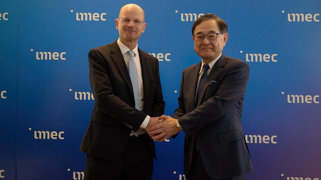
Imec, a global centre for advanced semiconductor research and innovation, is expanding its activities in Hokkaido, Japan, with the backing of Japan’s Ministry of Economy, Trade and Industry (METI) and in collaboration with the Leading-edge Semiconductor Technology Center (LSTC), to support the development of next-generation semiconductor and photonics technologies. As part of this expansion, imec is building a local R&D team, reinforcing its long-term commitment to Japan’s semiconductor ecosystem. The initiative will facilitate knowledge exchange and joint research activities between the two regions.
Growing collaboration across Japan
Building on imec’s growing collaborations across Japan and with Hokkaido as a rapidly emerging centre for semiconductor innovation in Japan, the new presence reflects the increasing importance of photonics and co-packaged optics (CPO) technologies as the industry seeks more energy-efficient solutions to support future AI and high-performance computing systems. Fully integrated in imec’s global R&D activities, imec Japan’s Hokkaido R&D centre will support national photonics-related research programs and foster collaboration between leading Japanese universities, research institutes and industry partners. To support these activities, imec intends to grow a local R&D team in Hokkaido to approximately 15 researchers and engineers over the next five years, while creating strong collaboration links between teams in Hokkaido and Leuven. The team will be based on the Hokkaido University campus in Sapporo, Hokkaido, forming imec’s R&D base in Japan.
The Hokkaido-based team will work closely with organisations including Hokkaido University, Tohoku University, Yokohama National University, National Institute of Advanced Industrial Science and Technology (AIST) and Chitose Institute of Science and Technology to advance cutting-edge photonic integrated circuit (PIC) and electronic-photonic integrated circuit (EIC) technologies. These innovations are expected to play an important role in enabling future semiconductor systems and supporting the commercialisation efforts of industry partners, including Rapidus Corporation, a Japanese advanced semiconductor manufacturer.
Patrick Vandenameele, CEO of imec: “Japan plays a vital role in the global semiconductor ecosystem, with world-class expertise spanning materials, equipment, manufacturing and research. Through our R&D activities in Hokkaido, we aim to contribute to Japan’s ambitions in next-generation semiconductor and photonics technologies while further strengthening the connection between Japanese innovation and our global R&D ecosystem. By bringing together leading universities, research institutes and industry partners, we can accelerate innovation on common ground and help create the technologies that will power future generations of AI and digital infrastructure.”
Joint projects
Kiyohiro Houkin, President of Hokkaido University: “After signing an LOI in November 2024, Hokkaido University and imec proposed joint projects for co-packaged optics R&D in semiconductors, advanced packaging and medical AI use-case expansion, both of which kicked off this year. Training for our graduate students at imec has also begun. In the very year Hokkaido University celebrates its 150th anniversary, we are truly proud that our campus has become home to imec’s first R&D base in Japan. Looking ahead, I hope this opportunity will accelerate the flow of talent and strengthen semiconductor partnership between Japan and Europe.”
The initiative complements imec’s broader engagement with Japan’s semiconductor ecosystem, where the organisation has collaborated for many years with leading companies, universities and research institutes. By combining imec’s expertise, world-class R&D infrastructure and global partner network with Japan’s growing semiconductor ambitions, the collaboration aims to accelerate innovation and strengthen international cooperation in strategic technologies.